Research Directions
The Neuromorphic Device Lab studies device concepts that connect semiconductor materials, memory physics, sensing, and energy-efficient computing. Our work emphasizes experimentally grounded device characterization and application-aware neuromorphic functions.
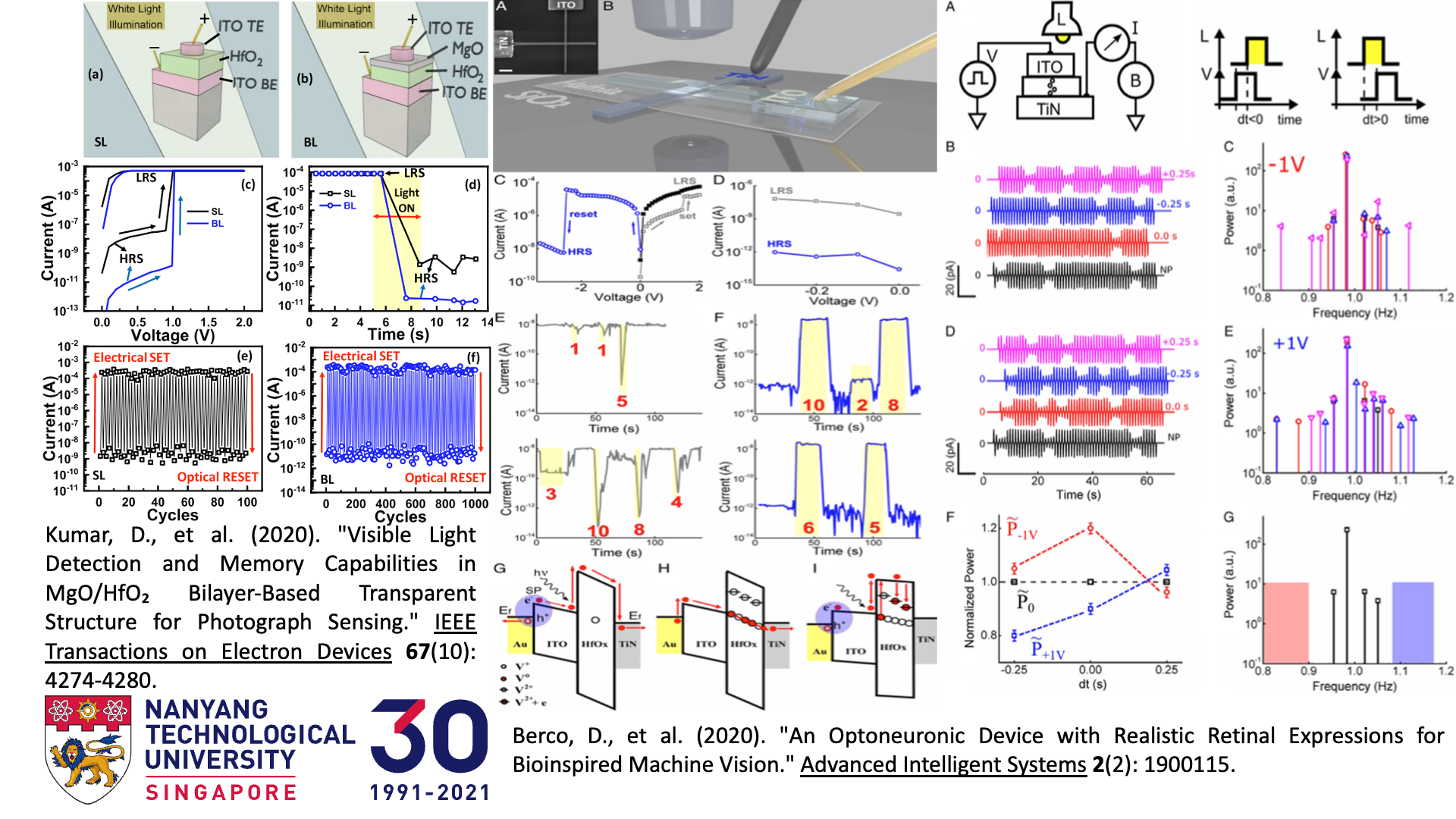
Retinomorphic Vision Sensors
We develop bio-inspired optoelectronic devices and sensor concepts for dynamic machine vision, visual memory, and energy-efficient front-end processing.
Related work: Nano Research 2025; Advanced Intelligent Systems 2021; Advanced Intelligent Systems 2020.
CBRAM and RRAM Devices
We investigate conductive-bridge and resistive switching devices for high-density memory, selectors, synaptic functions, and in-processor integration.
Related work: ACS Applied Electronic Materials 2024; Applied Physics Letters 2023; IEEE Electron Device Letters 2023.
Neuromorphic Memory Devices
We study memory and transistor structures that emulate synaptic and neuronal behavior, including plasticity, leaky integration, and device-level learning functions.
Related work: Nanoscale Horizons 2023; IEEE Electron Device Letters 2022; ACS Applied Materials & Interfaces 2020.
High-k Reliability And Trap Dynamics
We characterize charge trapping, gate dielectric reliability, hot-carrier effects, and nanoscale variability in advanced transistor and memory devices.
Related work: IEEE Transactions on Electron Devices; IEEE Electron Device Letters; Journal of Applied Physics.
Methods And Capabilities
- Electrical characterization of memory, selector, and transistor devices
- Reliability testing and trap dynamics analysis
- Device physics interpretation for neuromorphic and sensing functions
- Collaboration with industrial and academic partners on emerging semiconductor devices
Related Pages
See Publications for the full publication list, People for current members, and Join Us for student and collaboration opportunities.